
Preamplifier Prototype I
- PCB Layout and Schematic – PCB • SCH
- Photos of prototype: Photo 1 • Photo 2 • Photo 3 • Photo 4
Prototype passed a signal, though not without an oscillation at ~350MHz. Pictured is the result of sending a 500mV square wave with a 1ms period and a 10% duty cycle.
Preamplifier Prototype II
- PCB Layout and Schematic – PCB • SCH • PDF
- BOM – PDF • CSV
- PCB Photos: Front • Back
New PCB layout uses a 4-layer board design, and strictly adheres to board layout suggestions in TI datasheets for both the OPA847 and THS3201. This design does not oscillate. A -200mV DC offset exists when the test pulse cable is connected. If undesirable, can be corrected with a simple offset nulling circuit connected to U1-3 (non-inverting input of OPA847).
Update: 9/26/2011 An oscillation has been discovered at 700MHz with a peak to peak voltage of ~120mV. Removal of the .36pF capacitor (C3) in the feedback loop of the OPA847 solves this problem. Smaller oscillations still exist at ~20mV at close to 100MHz, and are currently being addressed.
Update: 9/28/11
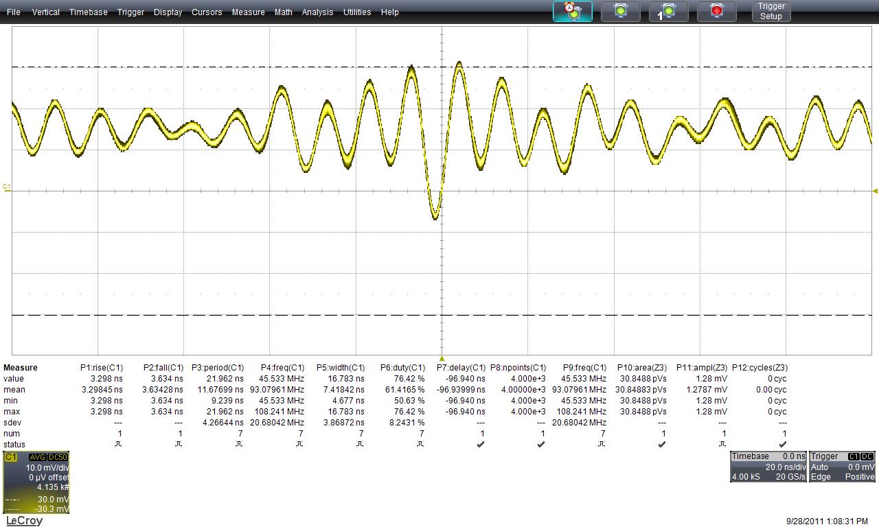
- Oscillation at ~100MHz with 2nd opamp disconnected (R11 removed)
- 100 ohm resistor was placed in series between the output of the photodiode and input of OPA847 (U1-2).
- 10pF input pic
- 100pF bypass capacitor added in parallel to both power supplies
10pF input pic 1 pic 2 pic 3
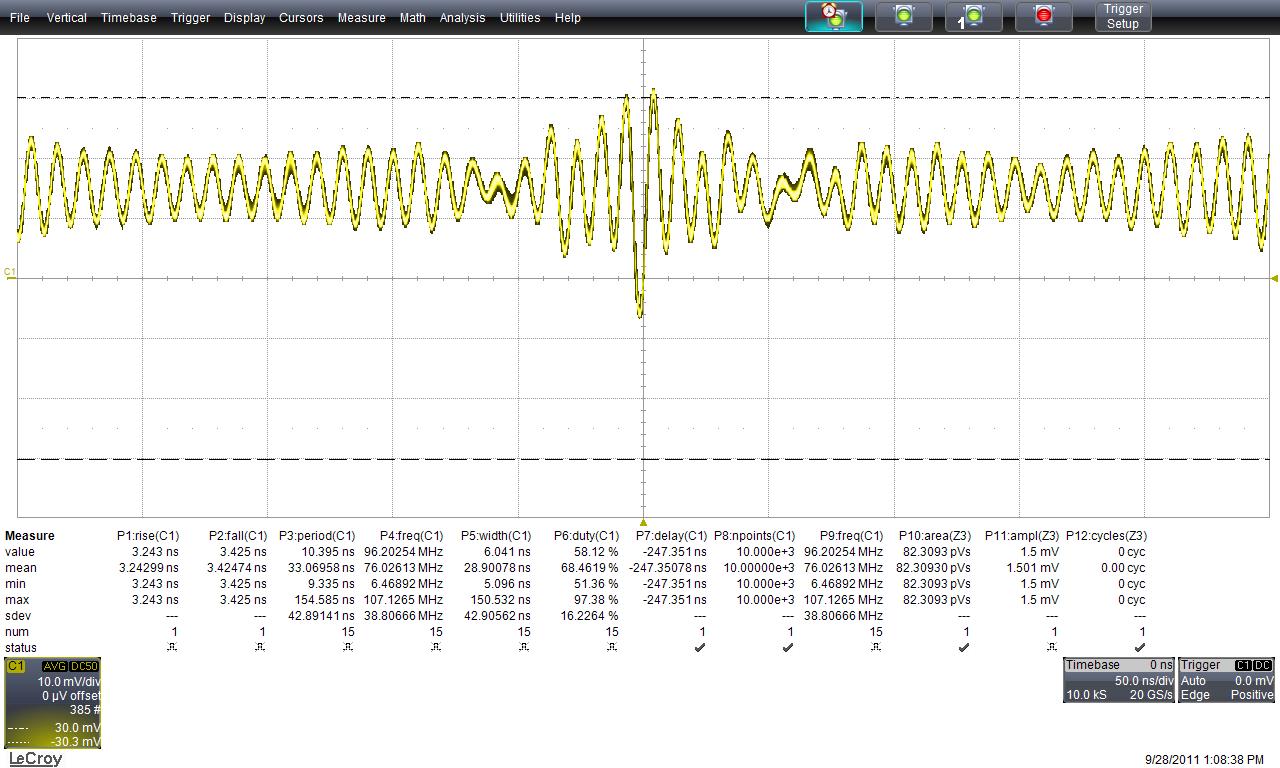
- R11 changed to 4k - severely decreased oscillation, added 30mV offset.
CompactPCI Power Board
The CompactPCI Power Board is a two slot wide 6u cPCI backplane that provides ATX power and RS232 breakouts for a single XCalibur 4301 module. Please note that on the version 1 board the ATX 5VSB is connected to ATX 5V. This will prevent the ATX power supply from starting up. Therefore you must not supply the 5VSB to the version 1 board. It is recommended to cut the 5VSB wire ATX pin 9 purple (see http://en.wikipedia.org/wiki/ATX#Power_supply). This problem is resolved in version 1.1.
- cPCI_backplane_v1.1.dxf
- cPCI_backplane_v1.1.zip
- cPCI_backplane_v1.zip
- cPCI_backplane_v1_BOM.xlsx
The original idea was to design a one-slot backplane-like board which would hold two connectors to mate with the J1 and J2 CompactPCI connectors on the processor board to supply power.
Other Documents
- ADC3925 User Manual
- EVI_ReceiverAmpCircuit.pdf
- SBOA122
- Photodiode Amplifiers
- DWEL-1.ods
- G8376
- OPA847
Design Notes
ADC3925 input is 50 ohms, 0dBm full scale (225mV). 10 bits implies 0.2mV or so LSB.